MicroStencil Dual Layer Stencils
The MicroStencil Dual Layer foil is ideally suited for fine dimension high tolerance printing. The stencils are fabricated through a two step lithography and Ni electroforming process with precise alignment achieved between the two layers. This process enables the deposition of lines down to 50 microns wide. The lifetime of the MicroStencil Dual Layer foil is at least 10 times that of a screen. Such stencils are well suited for a number of different applications including:
- Printing the front and rear contacts for solar cell manufacture
- Depositing both the vias and the circuit layers for LTCC production in one printing step
- Printing fine feature low cost disposable electronics like the antenna circuit in RF-ID tags
- Flux printing
- Printing on to substrates containing a topography or raised feature
- Wafer backside coating
- Deposition of novel materials such as biological materials onto electrodes and receptors for life sciences applications
The MicroStencil Dual Layer technology is commonly offered in the patented DEK Vector Guard frame format which enables significantly improved dimensional accuracy, space saving benefits and ease of handling the foil when compared with the traditional mesh mounting process.


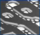
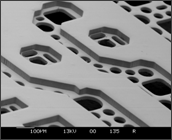
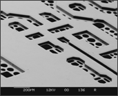
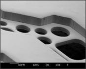
Electron microscope images of dual layer stencil features down to 50 micron wide lines
Benefits of Dual Layer Stencil technology
- High tolerance, fine dimension printing
- Lifetime of dual layer stencil is at least 10 times that of a screen
- The ability to print long conductive lines without the stencil losing structural integrity
- Stencil is easier to clean than a screen.
- Offset printing is possible with this type of stencil.
- The mesh layer of the stencil can be designed to accurately control the flow of paste to the second layer which is not possible with a conventional screen. MicroStencil have specialist CAD experience on designing this mesh layer
- The dimensional accuracy using the Vector Guard format is excellent (better than 0.1µm/mm)
Product Specifications
- Available thickness → 40µm to 200 µm in 0.5 µm increments
- Aperture capability → 35µm
- Aperture size tolerance:
- < 3 µm for 40-60 µm thick stencils
- 4 µm for 60 – 100 µm thick stencils
- 6 µm for 100 – 200 µm thick stencils
- Excellent thickness uniformity across design area +/- 5%
- Alignment between layers better than 10µm
- Positional accuracy → 0.2 µm/mm for traditional mesh mounting and 0.1 µm/mm for DEK Vector Guard format
- Pitch → 80µm
For enquires please contact: sales@microstencil.com
Back to products page

